Description
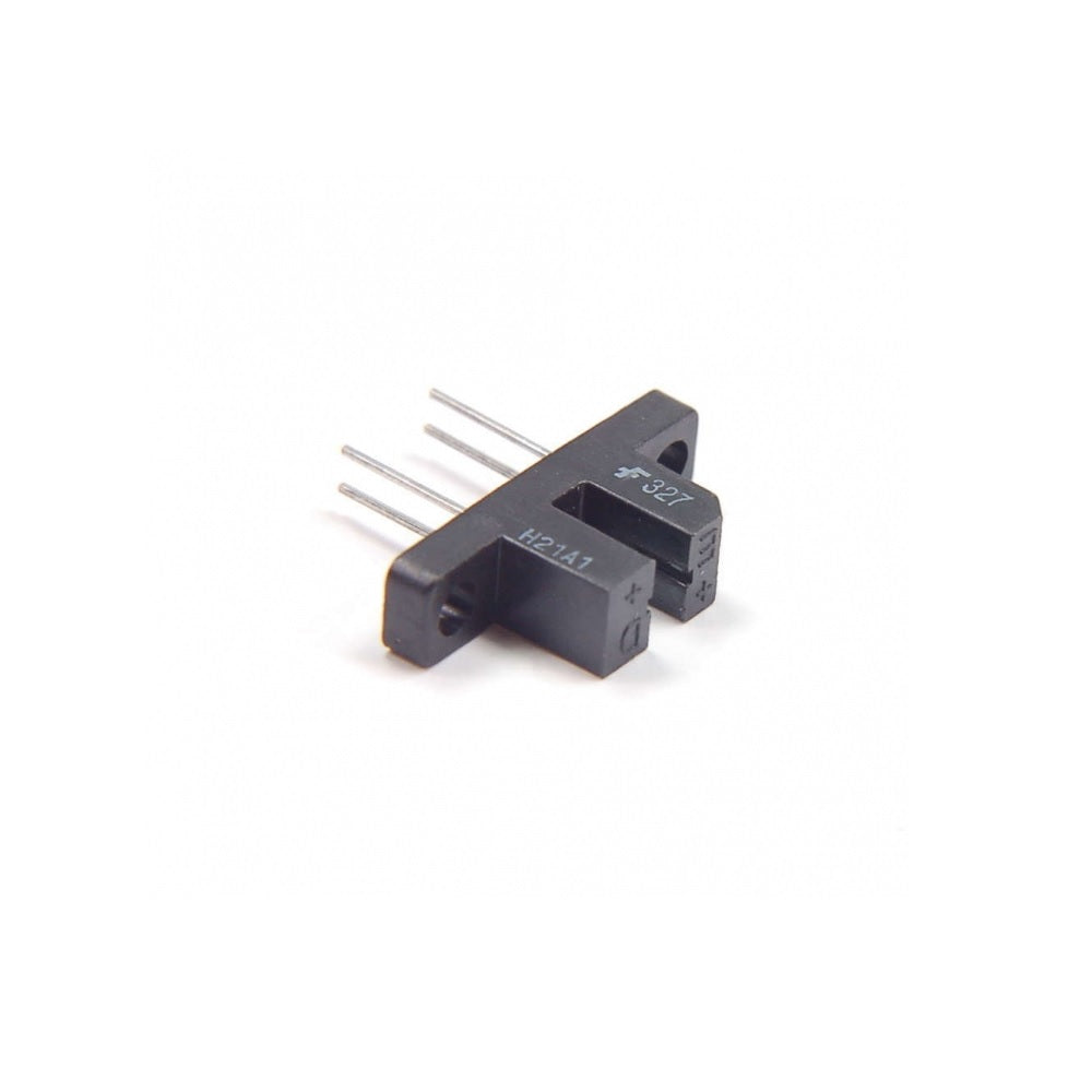
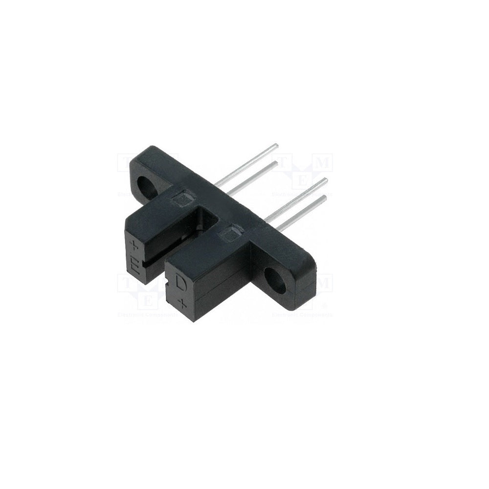
The H21A1 consist of a gallium arsenide infrared emitting diode coupled with a silicon phototransistor in a plastic housing. The packaging system is designed to optimize the mechanical resolution, coupling efficiency, ambient light rejection, cost and reliability. The gap in the housing provides a means of interrupting the signal with an opaque material, switching the output from an “ON” to an “OFF” state.
Technical Specification:
- Configuration: Photointerupter
- Peak Wavelength: 40 nm
- Gap Width: 3 mm
- Power Dissipation: 150 mW
- Maximum Collector Emitter Voltage: 30 V
- Maximum Emitter Collector Voltage: 5 V
- Maximum Collector Current: 20 mA
- Input Voltage: 1.2
- Maximum Forward Current: 50 mA
- Maximum Rise Time: 8 us
- Maximum Fall Time: 50 us
- Size: 24.7mm*6.35mm (L*W)
Features:
- Opaque housing
- Low cost
- .035” apertures
- High IC(ON)
Applications:
- Record players
- Optoelectronic switches
- Copier
- Printers


